TOP
I found some of the art work for some Power Amp PCB, I was messing about with to make some time.The Power Amp circuit design was based on a very basic amp design, that I used on one of my early disco decks back in the 1970's
I acutely found an old 19-inch rack case that I made, about 25 years ago, with two of these basic amps in, with their power supply, and they still worked. Their not what I would say are HI-FI but they work with a reasonable band width up to 15Khz, with 50 Watts RMS.
(I think that by looking at the holes on the back panel there was going to be six amps in here, may be high, mid and low, each side for stereo.)
There was even a multi input mixer pre amp in a 19-inch 1 U panel to go with this, God knows where that ended up, if I can remember properly, it had a couple of microphone input and two pick up in put, with tone controls.
I know this amp system was use a few times by a comedian, at a club some where in Essex, back in the 1980's.
Hot News
~~~~~~~~~~~~~~~~~~~~~~~~~~~~~~~~
*********************************************************************************
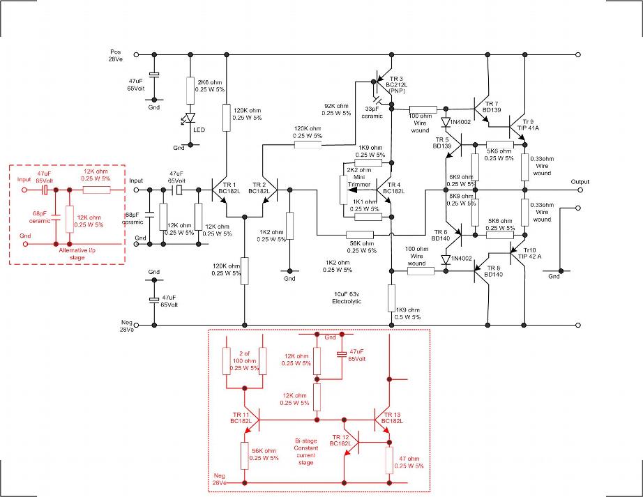
* I've back tracked the PCB lay out and drawn out the circuit diagram for this Power Amp Board. *
* (9 June 2011). *
* The circuit diagram is lower down this page, and I will be discussing a number of simple *
* changes to this board, to improve it a little. *
********************************************************************************
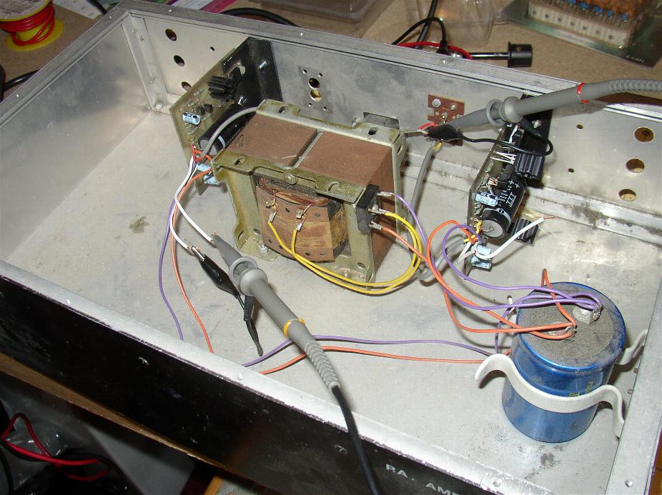
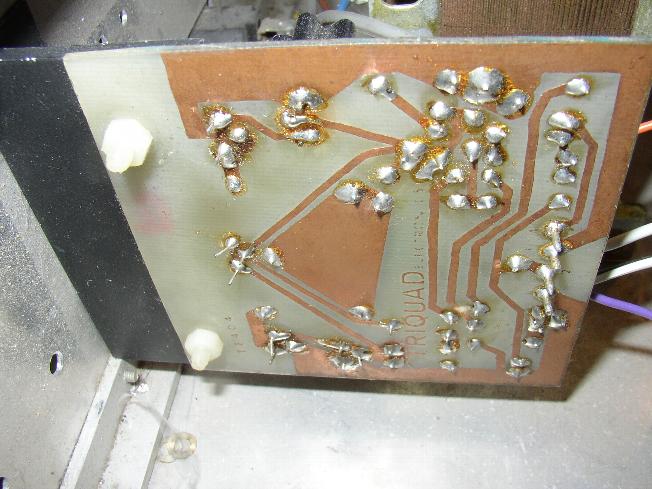
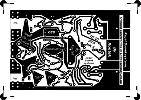
The 19 inch rack mount P.A. Amplifier which was badge under TRIQUAD Electronics.
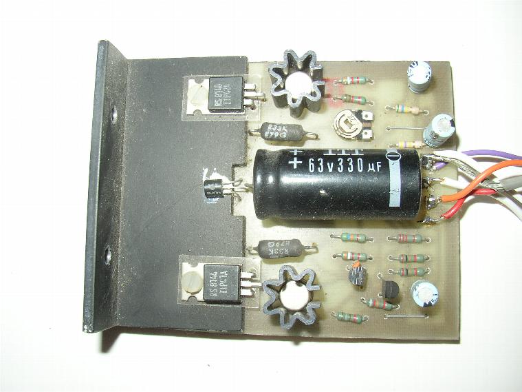
One of the populated printed circuit boards, notice the output pair and the temperature compensation transistor in the middle, mounted on the heat sink, the small variable
resistor is for adjusting the bias voltage across the two output transistors. The two smaller metal can medium power driver transistor, have a small clip on heat sink.
As the circuit works on a single supply voltage of about 55Volts DC, the need for the big output capacitor is nicely mounted down the middle of the board.
The other two small plastic signal transistors act as the input circuit and the voltage gain stages, to produce the 23.5 volt peak (or 47 volt peak to peak signal) from an
input signal of about 1 volt.
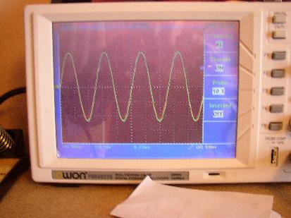
My digital scope, showing the out put wave form, with a 800mv pk input at 1.5 Khz, displayed on the scope in red (which is terrible to see), the output is in yellow
(a much better colour to see.) this was just before its max voltage swing (where it clips the peaks) at 47 Volts peak to peak.
This is the maths bit half sig = 23.5
Volts^2 = 552.25 (volts squrared) \
watts = ---------- = ----------
Divided by >
= 69.03125 Watts peak, then divide by 1.414 to get RMS which = 48.81984 Watts
ohms = 8
( 8 ohm speaker) /
Which is not bad for a little board which must of cost me about a tenner £10.00 or $15.00. the most expensive item must of been the transformer .
The printed circuit board was a home etched one, the heat-sink is a piece of L angle aluminium.
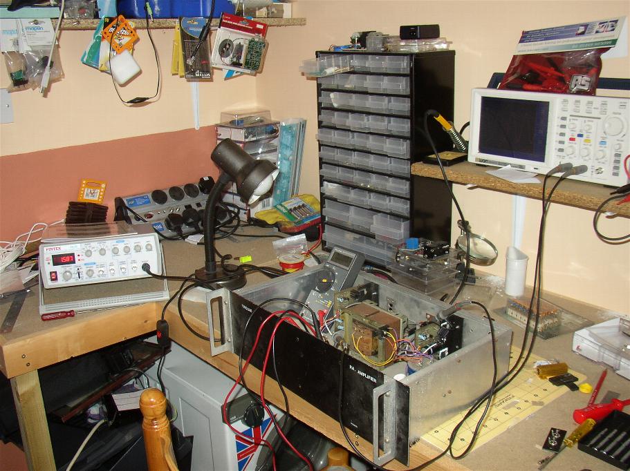
This is a tidy view of my work bench, with the amp under test.
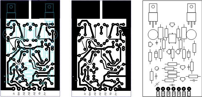
MK 2 board 50 watts RMS
I'v come across this Visio drawing of what I think is an up rated version of my basic power amp but i can not find the circuit diagram.
12 June 2011 I've just redrawn the circuit diagram for the above PCB layout Bd. and I found that one of the diodes on the layout was, the wrong way around.
I just need to make the PCB now and try it out.
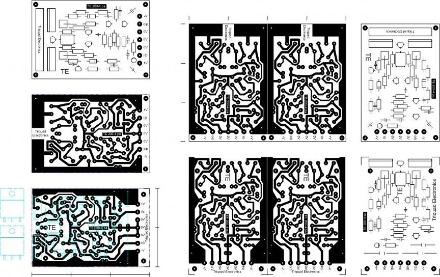
Some different lay outs these must be for a pair of darlington out put transistors ( a darlington is a single device that has two transistors inside one being the driver and the other a power output in an emitter follower configuration ie the emitter of the driver directly fed to the base of the output power transistor)
These look like a board lay out for some high power amps still based on the basic power amp design.
There will be some power amps of hi-fi specs to come soon. All I've got to do now is to back engineer, the above PCB lay outs, to come back with the circuit diagram's.
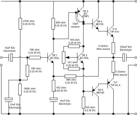
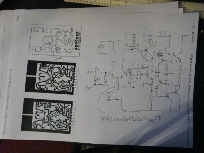
I did a bit of reverse engineering, on the 50Watt power Amp board, and I came back with this little circuit. It may look strange and very simple to some Hi-Fi experts,
but it works I don't think you can take it any higher than 50 watt / 55 volt power line swing though. I think you could increase the frequency top end from 15 - 20Khz
up a bit more by employing, some frequency compensation, in the neg feed back net work, and increase the 10uF caps up to 47uF or even 220uF. It worth a try?
The centre pot (Variable resister) is a 2 K mini trimmer, this needs to be adjusted so you get 2.8 volts across the base of TR 4 and the Base of TR 5, this will forward bias the output stage just enough to stop transistor cross over distortion, when the output transistor switch on, on ever half cycle.
N.B. TR3 should be heat bonded, on to the same heat sink as the two main output transistor, this is for heat feedback to stop thermal run away. This will trun down the
out put transistor the hotter they get, as the heat turns TR3 on more thus reducing the biasing voltage so turning the driver transistor down.
Back to top
NB: just check made bd and I got
the value of the small ceramic cap across the base / collector of TR2 it
should be 33pF, I thorough it was a bit high value. this cap acts as
internal circuit local voltage stage NFB, this stop oscillation and rf
noise.
NFB are the negative feed back additions to increase the upper frequency response.
NFBCx will reduce the resistance at around 15Khz as the gain is calculated by the 56k resister divided by the 1k2 resister with out the capacitors it gives a circuit
gain of about 48, but with the cap Cx reducing it impedance with frequency, it reaches 1k2 at about 15Khz which will start increasing the gain as with a low value to
divide 56K with will get a higher signal gain. if done a quick calc of Cx and it came out at around 8.8nf you could use a 6.8nF up to 10nF
NFBCy will kick in at about 50Khz, to stop the gain and phase shift from taking the circuit in to oscillation. I calc Cy to about 2.6nF try a 2.2nF
The Elec 47uF cap across the tr bias circiut, just acts as a signal bypass to the DC biasing. And the addition of the 100nF cap on the supply rail, just acts to reduce
any local rf noise on the supply rails.
1 1 1
Cap impedance = ---------------------------- or Cap = -------------------------- = ----------------------- = 0.000000008832 = 8.8nF
2 pi x frequancy x Capacitance 2 pi x frequancy xresistance (2 x 3.145) x 15Khz x 1200
11 June 2011
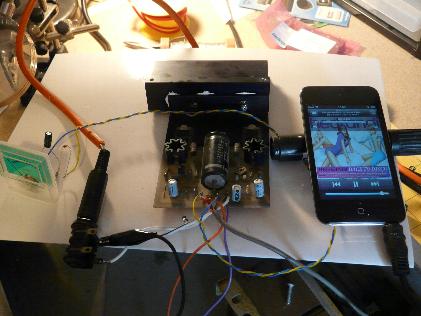
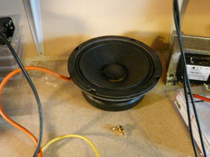
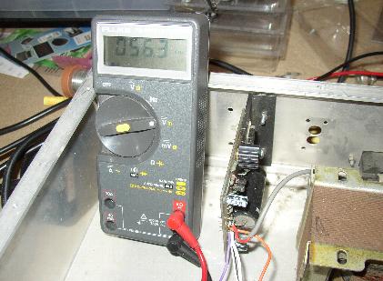
Before I made any changes, I thought I would give it a try connected to a MP3 player and connected to a 6 inch 8 ohm 200 Watt speaker.
The sound quality suprised me, It was quit good, it was good enough for disco work. As you can see from the scope image below.
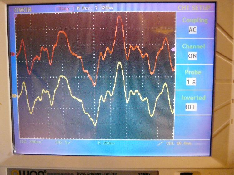
This was a captured part, of the music waveform, the input is in red (top waveform), the settings was 200mV per div giving a i/p of about 820mv pk to pk.
The lower Yellow waveform is the output, the setting is 5v per div giving a o/p of about 20 Volts pk to pk. As you can see there is little difference in the two waveforms, they are in phase with no phase shift.
I also connected it to the signal generator, to find the frequency were the output dropped to half the value, with the same i/p level at 1.5 Khz. I was suprised to find at the -6db level was at about 60 Khz from the unchanged circuit. That little £10.00 board supprised me it has quit a lot of punch per £1 compaerd to the professional bought amps I have of about £250.
Back to top
MK 2 board 50 watts RMS
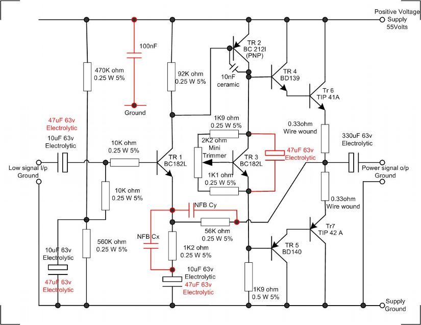
Redraw circuit diagram of Mk 2 50 W RMS board, with additions / changes in Red. I need to redo the transparncy art work for board etching to take in account the changes.
Hot News Dated 6th July 2011 ( error in above circuit Sorry).
The collector of TR 2 should not go directly to the base of TR 3, as the returned NFB will be the wrong phase thus giving Positive feed back not negative,
so circuit would try to Oscillate.
There should be another transistor in between. Amended circuit and PCB track work to follow shortly.
The track art work for Mk 3 50 watt power amp board. With changes implemented.
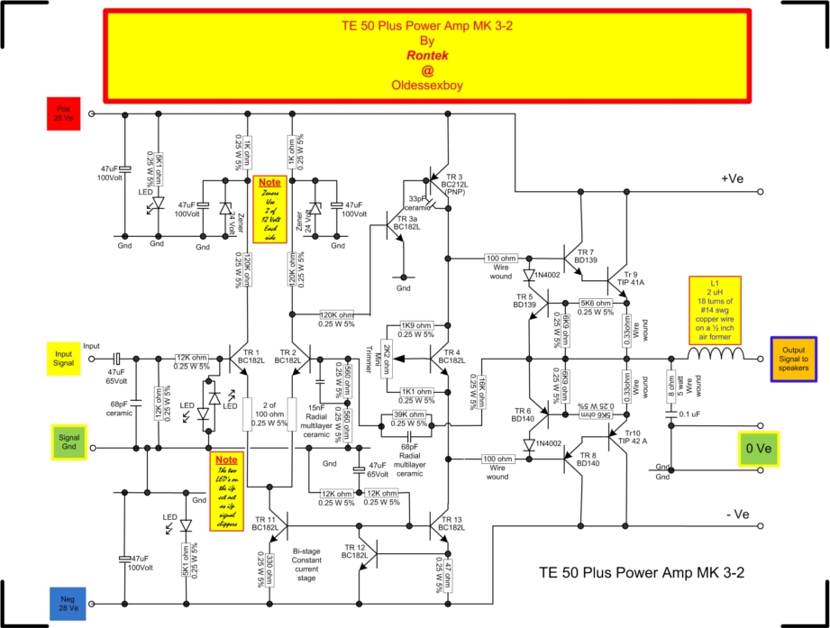
The Circuit diagram for Mk 3 50 watt power amp board. With changes implemented.
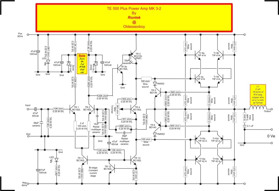
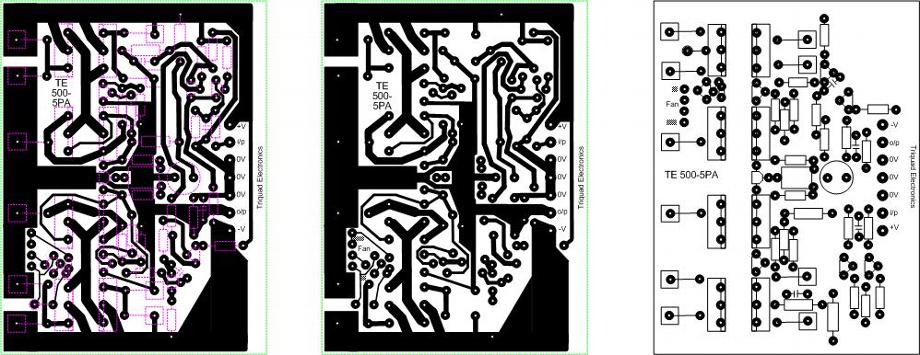
The Circuit diagram for Mk 3 500 watt power amp board. With changes implemented.
NOTE:- the out put power transistors, are darlingtons.
The top four NPN's ( Tr 9 ( a-d)) could be TIP 142 each being Vceo 100 volts, Ic 10 Amps, 125 Watts, hfe 500 - 1000
The Bottom four PNP's ( Tr 10 ( a-d)) could be TIP 147 each being Vceo 100 volts, Ic 10 Amps, 125 Watts, hfe 500 - 1000
This will give an output ciruit that can cope with an output swing of 200 volts, and 20 Amps
with the +80 Volt, 0 volt, -80 volt supply we get :-
with a 8 Ohm load speaker, 80 squ'd = 6400 / 8 ohm = 800 watts pk giving 10 Amps ( 565.6 Watts RMS )
with a 4 Ohm load speaker, 80 squ'd = 6400 / 4 ohm = 1600 watts pk giving 20 Amps ( 1131.2 Watts RMS )
but you will not get the full supply swing, but it best to calculate the MAX.
You may only get 75 volts on the output but that will be OKay.
That gives 703.125 Watts pk with 8 ohm load (497.1 watts RMS)
or
That gives 1406.25 Watts pk with 4 ohm load (994.22 watts RMS)
To cope with the 20 Amps there needs to be some changes to the protection Resistance network.
The output Wire wound 0.33 ohms dropped to 0.1 ohms which give 2 volts across it, so the 5k6 needs to be about 13K ohms.
~~~~~~~~~~~~~~~~~~~~~~~~~~~~~~~~~~~~~~~~~~~~~~~~~~~~~~~~~~~~~~~~~~~~~~~~~~~~~~~~~~~~~~~~~~~~~~~
This free script provided by
JavaScript
Kit